In today’s fast-paced electronics industry, delivering high-performance printed circuit boards (PCBs) requires more than just a great schematic. It takes careful planning, iterative testing, and a strong understanding of multilayer design principles. Two of the most critical factors in this process are PCB prototyping and PCB stackup planning. Together, they lay the foundation for signal integrity, thermal reliability, manufacturability, and long-term performance.
Why PCB Prototyping Matters
Before entering mass production, it is essential to validate your design through a PCB prototype. Prototyping allows engineers to detect design flaws early, test functionality under real-world conditions, and iterate quickly without the risk of large-scale failure. Whether you’re developing a new consumer device or a complex industrial controller, a well-built prototype is your first line of defense against costly design errors.
PCB prototypes also help verify layout constraints, component placement, impedance control, and thermal performance. With fast-turn PCB design services, you can evaluate multiple layout variations and move your project toward a production-ready board with confidence.
Understanding PCB Stackup Design
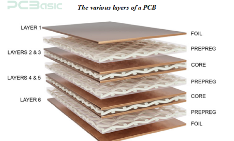
Once your initial layout is validated, the next step in optimizing performance is designing the correct PCB stackup. The stackup refers to the arrangement of copper layers and dielectric materials in a multilayer PCB. This structure significantly affects impedance control, EMI shielding, signal integrity, and power delivery.
A well-engineered PCB stackup:
- Minimizes crosstalk between signal layers
- Controls trace impedance for high-speed signals
- Provides a solid return path for ground and power
- Reduces radiation and susceptibility to noise
- Enhances mechanical strength and thermal performance
For high-frequency and multilayer designs, improper stackup selection can result in degraded signal performance, excessive power losses, and EMI compliance issues. That’s why early collaboration between electrical and manufacturing teams is essential.
Integrating Prototyping and Stackup for Best Results
While prototyping and stackup planning are distinct steps, they are deeply interconnected. A prototype without a realistic stackup might pass initial tests but fail under production constraints. Likewise, an optimized stackup with no real-world testing cannot guarantee functional performance.
At PCBasic, we integrate PCB design, prototyping, and stackup consulting to help clients achieve faster development cycles and more reliable final products. Our engineering team works closely with customers to align layout goals, signal integrity targets, and fabrication capabilities from the very beginning.
Conclusion
Optimizing PCB performance is a strategic process that starts well before the first board is assembled. By investing in high-quality PCB prototypes and carefully planned PCB stackups, designers can minimize risk, ensure functional accuracy, and maximize product success.
Whether you’re working on a high-speed communication system, a compact wearable, or a robust industrial controller, remember: the path to performance starts with prototyping and stackup done right.